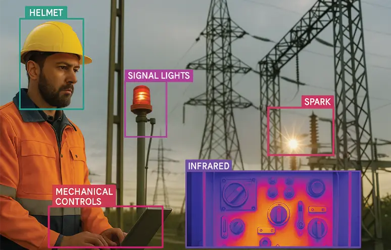
Sub-5nm defect detection remains one of the biggest yield challenges in semiconductor manufacturing. Traditional optical and electrical methods struggle with the complexity and feature size of modern chip architecture. When such defects go undetected, they lead to yield loss, delays, and rework. To stay profitable at advanced nodes, inspection needs higher-resolution imaging and smarter decision-making at the right steps in the process.
Machine learning addresses this gap across the manufacturing flow. As Ajay Baranwal, director of the Center for Deep Learning in Electronics Manufacturing (CDLe), notes:
“Analyzing high-dimensional semiconductor material properties, and predicting which material meets the desired specifications and characteristics, are being done using ML algorithms for material selection. Defect detection and classification for semiconductor wafers and masks have shown promising results. Offline and real-time process monitoring and control are used too.”
A machine vision application in semiconductor manufacturing delivers this capability by combining calibrated optics, controlled lighting, and AI-driven models.
This blog post covers how machine vision fits across the wafer-to-package flow, why it is essential for quality control, which semiconductor inspection system types to use for different stations, and the measurable benefits you can expect in yield, rework, and cycle time. We will first start with an overview of semiconductor manufacturing.
What is semiconductor manufacturing?
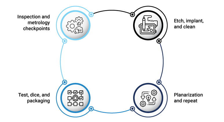
Semiconductor manufacturing turns ultra-pure silicon into finished integrated circuits through precisely sequenced steps in the fab and the back end. The front end builds transistors layer by layer on the wafer, while the back end isolates functional dies, assembles them into packages, and validates their performance. A semiconductor manufacturing process can involve hundreds of steps. The exact number depends on the chip’s complexity. Advanced designs can involve more than a thousand steps, each sensitive to contamination and variation.
Wafer preparation and films
Silicon ingots are sliced into wafers, and thin films are then deposited or oxidized to build the base stack. At this stage, ensuring clean and uniform surfaces helps reduce defects and rework later in the process.
Photoresist coating and patterning
Photoresist is applied and exposed to define circuit features. Precision alignment ensures each new layer lands on top of the last without unwanted connections or breaks, preserving device performance.
Etch, implant, and clean
Etch removes selected material while ion implantation sets electrical properties. Thorough cleaning after each step prevents residues and particle additions that can compromise later layers.
Planarization and repeat
Chemical mechanical polishing levels the wafer surface so the next layer prints correctly. This build and polish cycle repeats many times to create the device.
Test, dice, and packaging
After an electrical test, the wafer is cut into individual chips. Good chips are mounted on a substrate or leadframe, connected, and sealed. Advanced packaging (for example, interposers and high-bandwidth memory) adds many more connections and raises reliability needs.
Inspection and metrology checkpoints
At key points, optical, electron-beam, and other modalities verify patterns, dimensions, and defects to keep the flow in spec. For faults that are difficult to identify, parallel electron-beam inspection is used to accelerate defect detection.
Semiconductor manufacturing relies on precise control across these stages, which makes high-yield inspection a critical part of the process. Well-placed checkpoints provide quick feedback, so issues are addressed as soon as they are flagged, and good quality units proceed to final testing and shipment.
Why is quality control important in semiconductor manufacturing?
Quality control in semiconductor manufacturing protects product performance and reliability before chips ship. It also reduces rework that can delay production and delivery.
Teams gain timely proof that each new layer is printed in the right place and that the tiny wiring and solder joints inside the package are sound. This confirmation happens before more time and materials are added, so issues are fixed when they are easier to correct.
Through quality control, you can:
-
Cover what electrical tests miss
Some defects, like microscopic cracks and dimensional variations, are difficult to spot quickly using only electrical tests during production. Add machine vision at the steps where defects arise to catch them early and prevent rework or scrap.
-
Use data to limit additional stress testing
Use data from earlier checks to pick out the few devices that still need stress testing. Let the rest continue through production to shorten cycle time and avoid unnecessary stress on good devices.
-
Find hidden package issues without cutting parts open
Problems like voids or peeling can start below the surface. Non-destructive ultrasound inspection checks every unit for these risks before stacking or shipment, preventing end-of-line scrap.
What are the common quality control challenges in semiconductor manufacturing, and how can machine vision help?
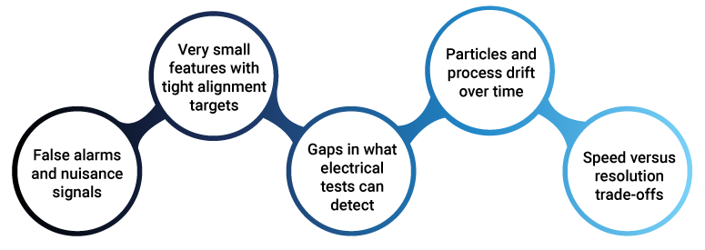
In semiconductor manufacturing, quality control needs to balance speed, precision, and yield. Each wafer contains billions of tiny features, so small misses can lead to costly failures. The challenge is to filter normal variation, find hard-to-detect defects early, and do it at line speed. The points below outline these challenges and how machine vision inspection addresses each of them.
-
False alarms and nuisance signals
Natural texture, pattern changes, or harmless marks can look like defects and generate too many alerts.
Solution: Implement AI classification on top of rule-based checks to filter variation, lower the review load, and focus action on real defects. -
Very small features with tight alignment targets
As dimensions get smaller, tiny placement errors can create shorts or opens. Keeping layer-to-layer alignment consistent across shifts, tools, and temperature changes is difficult.
Solution: Use vision-guided alignment and overlay monitoring that read fiducials and wafer notches precisely, track overlay in real time, and apply small corrections for stage and temperature effects. Routine calibration closes the loop, so layers stay within spec from across batches.
-
Gaps in what electrical tests can detect
Electrical screens can miss issues in thin surface wiring and in small connections between stacked parts, especially early in the flow.
Solution: Add targeted inspection steps where electrical tests are weak, using optical to catch surface defects, infrared or acoustic to reveal subsurface voids and delamination, and X-ray to expose hidden interconnect problems. With that coverage defined, apply 100% checks at high-risk steps and use sampling elsewhere with clear acceptance limits, so defects are found at the right time and place.
-
Particles and process drift over time
Sub-micron particles or small chemistry shifts can seed defects that appear several steps later, increasing scrap and delay.
Solution: Set frequent inline checkpoints and trend key metrics so small shifts are caught early. Study the reported trends and trigger clear actions when thresholds are crossed, such as adjusting the recipe, scheduling tool maintenance, or quarantining lots, so issues are contained before they reach later steps.
-
Speed versus resolution trade-offs
High throughput can blur fine details, while slower, higher-resolution imaging can slow down your production lines.
Solution: A well-tuned semiconductor inspection system can balance image quality with line speed and use smarter screening to focus attention on real risks.
Together these challenges explain why modern programs need to combine better imaging, precise alignment control, and AI-assisted classification to reduce false alarms, catch defects earlier, maintain line speed, protect yield, and ship reliable product on schedule.
What are the different types of machine vision systems in semiconductor manufacturing quality control?
There are different types of machine vision systems that use combinations of optics or sensors, motion control, and analytics to find defects and verify dimensions at line speed. The main inspection system types include optical, parallel electron-beam, X-ray, infrared, and scanning acoustic microscopy. Each serves a specific role from wafer build to advanced packaging, depending on defect type, coverage needs, and line speed.
-
Optical inspection and metrology (2D/3D)
The system uses high-throughput cameras and gauges to check surfaces, patterns, and dimensions on wafers and packages. In advanced packaging, optical inspection provides very high coverage at line speed for features that light can reach, while X-ray, acoustic, or infrared methods cover areas that optics cannot.
-
Parallel electron-beam inspection
For very small or electrically linked defects, electron beams provide higher sensitivity than optics. SPIE (Society of Photo-Optical Instrumentation Engineers) reports multicolumn approaches that target an order-of-magnitude throughput gain over single-column e-beam, accelerating defect learning during ramps without naming a specific vendor or beam count.
-
X-ray and Computed Tomography (CT)
X-ray imaging penetrates metals and underfill material to detect voids, misalignments, wire-bond issues, and hidden opens/shorts in flip-chip and BGA packages. As packages grow more complex, X-ray inspection is becoming essential at selected steps, with 100% coverage where the risk justifies it.
-
Infrared (IR) imaging and thermography
Because silicon passes certain IR wavelengths, IR can detect subsurface cracks and delamination in wafers and bonded stacks that surface optics miss. IR is increasingly used inline for bonded-wafer and stacked-die checks.
-
Scanning Acoustic Microscopy (C-SAM)
Ultrasound finds voids and peelings inside packages without cutting parts open. Industry sources describe SAM as an industry-standard choice for 100% inspection of subsurface risks, and it is expanding to hybrid-bonded devices.
When coverage gaps exist (for example, connections inside interposers and fine wiring above the wafer), semiconductor engineering industry guidance favors complete coverage using inspection and metrology to prevent escapes. Use optical for speed, add IR or C-SAM for hidden risks, and apply parallel e-beam during ramps or for the hardest defects.
What are the benefits of using machine vision in semiconductor manufacturing?
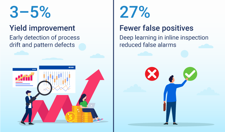
Source: MDPI, Keyence
The benefits of machine vision in semiconductor manufacturing are higher first-pass yield, steadier quality, faster ramp to volume, and more reliable semiconductor production line automation. Machine vision improves defect detection, alignment, measurement, and traceability across wafer fabrication and final assembly, delivering measurable semiconductor yield improvement with machine vision. Production teams realize the following gains:
-
Quality control and defect detection
Machine vision detects microscopic defects that can be missed during human inspection, including scratches, particles, and pattern anomalies on wafers and packaged parts. Because the same criteria are applied every time, results stay consistent, and issues are flagged in real time so teams can act immediately.
-
Efficiency and productivity gains
Machine vision inspects thousands of units per minute and applies the same pass or rework rules at production speed. It also automates repetitive tasks such as inspection, sorting, and measurement, which gives engineers more time for analysis and line improvement.
-
Cost reduction
Catching issues earlier increases yield and reduces scrap and waste. Preventing undetected defects from reaching later steps limits rework, returns, and warranty claims, which lowers total cost and keeps schedules intact.
-
Process optimization and traceability
Machine vision performs precise measurements, and alignment checks in both wafer fabrication and packaging. Each inspection generates traceable data for process tuning and predictive maintenance, and these signals can drive real-time adjustments that keep quality steady.
-
Specialized inspection capabilities
3D vision captures depth to assess heights, coplanarity, and stack geometry in advanced packaging. Hyperspectral imaging analyzes materials across many wavelengths to spot subtle contamination or material mix-ups that standard cameras cannot detect.
-
Automation that scales
When machine vision is embedded in tools and handlers, quality rules are applied the same way at each station and can be audited. This consistency supports semiconductor production line automation, maintaining throughput while keeping acceptance criteria clear and enforceable.
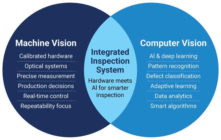
Machine vision vs computer vision: Their roles in fab operations
The difference between machine vision and computer vision is that machine vision is the factory-grade system that makes reliable pass, rework, or stop decisions on the line, while computer vision is the broader set of AI-driven technologies that learns patterns and helps classify what the cameras see. In fabs, machine vision is built for repeatability and uptime; computer vision strengthens it with learned detection and smarter classification.
-
Scope and purpose
Machine vision is the production system: calibrated optics, controlled lighting, timing with tools, and strict decision rules. Computer vision provides the learning layer that recognizes patterns and reduces false alarms across lots and tools.
-
How they work together
Machine vision captures and measures; computer vision analyzes those images to distinguish real defects from harmless variation. Together, they increase inspection coverage without slowing production and help maintain consistent outcomes across the shifts.
-
Layer alignment and overlay control
Layer-to-layer alignment has to be controlled at just a few nanometers to protect yield. For example, scanners from Nikon specify single machine overlay around 1.7 nm. That is why metrology and vision-guided alignment are core to production.
-
How an inspection system uses both
A semiconductor inspection system embeds machine vision for deterministic checks and uses computer-vision models where learned classification adds value, for example, in defect classification or nuisance-reduction.
Thus, machine vision runs your production line, while computer vision adds learning. In combination, they keep layers aligned, reduce false alarms, and keep output moving on schedule.
Reduce defects and improve yield with a machine vision system
Start small and prove value where it matters most. Set a clear target for one station or line: coverage, the highest acceptable false positive rate, and the allowed latency at line speed. Lock the imaging recipe, test it on the toughest parts, and log each decision (pass, rework, hold) so every step is traceable. Use a two-step flow: the first step runs a fast prescreen to mark regions of interest, and the second step performs a high-resolution check where needed, so you keep image detail while maintaining line speed.
With the right semiconductor inspection system, you can set clear acceptance rules, keep throughput steady, and make results auditable. A professional partner can help select the right tools, design lighting and optics for each station, and operationalize those rules on the line.
Talk to a specialist to review your current flow and build a focused plan to reduce defects and improve yield.
FAQs
1. How does machine vision improve alignment in semiconductor manufacturing?
Machine vision locates fiducials and wafer notches with sub-micron accuracy, compensates for stage error and thermal drift, and keeps layer overlay within spec at production speed. Add overlay SPC and in-tool feedback so small shifts are corrected automatically, reducing rework and stabilizing yield across lots and shifts.
2. Why is line scan technology used in semiconductor production?
Line scan technology is used in semiconductor production because it captures high-resolution images of moving surfaces without motion blur. The camera acquires one line at a time while motion encoders keep pixels evenly spaced, which makes tiny defects remain sharp at line speed.
3. How do you ensure the quality of vision systems for semiconductor manufacturing?
Define acceptance criteria upfront (coverage, false-positive rate, latency), verify Gage R&R, and validate throughput at line speed with representative data. Include a calibration plan and model maintenance to prevent drift. Talk to us about setting these gates for your line; we’ll map them to your stations and ROI targets.
4. How does AI contribute to machine vision systems?
AI contributes to machine vision systems by learning visual patterns from data to improve detection and classification while reducing false alarms. Deep learning separates true defects from normal texture or cosmetic marks, labels defect type and severity for faster root-cause analysis and adapts to new products with transfer learning so setup time is shorter.