Customer background

The client is a large-scale manufacturer and distributor of wafers used in the production of electronic devices like desktops, laptops, smartphones, televisions, washing machines, digital cameras, and refrigerators. They also offer diagnostic services and wafer customization services. They serve clients in the electronics, biotech, and nanotechnology industries. The company is operational since more than five decades and has its head office in the USA, and registered offices in China and Japan.

Challenges

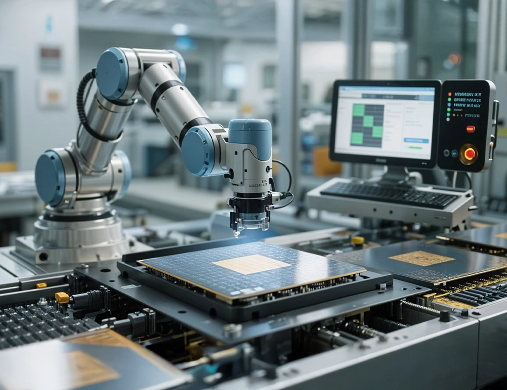
Semiconductor wafers are crucial in the electronic world because they serve as the base material for creating electronic components like transistors, resistors, and capacitors. Our client, being a leading provider of wafers, had to manufacture wafers in huge volumes. Defect detection is an important part of production as wafers must be checked for quality before rolling out. Our client struggled with:

Manual defect detection process - Their manual defect detection process was tedious, time-consuming, and prone to errors. This led to delays in production and affected order delivery ETAs.

Inefficient system – Their old system was not accurate in distinguishing relevant and irrelevant images. This resulted in poor quality production which slowed down their operational efficiency.

Inability to fulfill orders – As production was affected due to the above reasons, they were not able to fulfil the demands of their distributors and suppliers in time.

Solutions

Our team conducted thorough consultations with the client’s team. We proposed developing a backend solution using deep learning technology to identify defect patterns and perform image classification effectively. Our solution development process included:

Data analyzation

Our team analyzed the data to understand the root cause of the problem. We observed the position of defects in the wafer images at various locations which gave us insight into the common defect scenarios.

Preparing the dataset

We carried out the pre-processing of the data and applied the grayscale image segmentation technique. Our approach was to carry out detection as a classification task at the pixel level. Therefore, we created data models that examine background pixels and foreground pixels, which helped us to extract pattern features.

However, the client provided us with a limited set of data, and deep learning networks require a large amount of data for training. Moreover, in the case of semiconductor wafers where defects must not be frequent, the number of non-defected images outweighed the defected images.

Therefore, to resolve the imbalanced dataset problem and to enlarge the dataset, we carried out image augmentation with Keras Python Library. This helped us to increase the number of samples in our data set using the small data set provided by the client. Further, we divided the enlarged dataset into training and validation data.

Building the neural network model

We decided to use Google’s pre-trained TensorFlow Inception CNN Models instead of creating and training the deep neural nets from scratch to save time and data. Then we fine-tuned the weight parameters using the feature extraction mechanism which included feature creation, feature ranking and dimensionality reduction. We trained the new classification model written in Python on our dataset to identify defect patterns and predict the label of unseen wafer images in the future.

Validation and deployment

We evaluated the trained Python model on the new wafer images to calculate its predictive accuracy. Our solution achieved 99% defect detection accuracy, and we deployed it successfully to production on Nvidia GTX 1060 8GB GPU.

semiconductor-portfolio-diagram
  • Industry

    Semiconductor manufacturing

  • Technologies / Platforms / Frameworks

    Python, TensorFlow, Keras, Azure Blob Storage

  • Benefits

    • Improved accuracy of detecting defected wafer images
    • No human involvement or error with an automated system
    • Rare event detection capability using the deep learning approach
    • Reduced memory requirement using a convolutional layer
    • Visualized predictive analysis on images using a real-time dashboard

Decades of Trust & Experience

projects

1630+

Projects

technocrats

545+

Technocrats

product-and-solutions

26+

Products and Solutions

Customers

1020+

Customers

Connect Now

Our experts would be eager to hear you.