
The demand for faster, smaller, and more powerful chips is at an all-time high, driving the semiconductor industry into an era of rapid innovation. However, the conventional chip design techniques are struggling to keep pace with this growing complexity. This is where generative AI in chip design is making a significant difference. By merging the creativity of machine learning models with the accuracy of engineering, artificial intelligence chip design is opening smarter, faster, and more efficient ways to build semiconductors.
Unlike conventional processes that rely heavily on manual trial-and-error, AI for chip design can explore millions of design options, optimize layouts, and anticipate performance with phenomenal accuracy. From reducing design cycles to optimizing energy efficiency, AI in the semiconductor industry is enhancing productivity and changing the way chips are conceived and built. This transformation signifies that generative AI is a present-day solution that is shaping the future of semiconductor innovation.
What is generative AI in chip design?
Generative AI in chip design is the use of advanced AI models that can automatically generate, optimize, and validate semiconductor designs. Generative AI applies algorithms to explore design possibilities, simulate outcomes, and suggest improvements. This approach helps engineers create more efficient circuits, reduce design errors, shorten development cycles, and accelerate the path from concept to silicon.
For example, consider a scenario where, rather than having to spend months individually placing millions of pieces of equipment on a circuit board, an engineer simply types a brief request such as “design a 3GHz processor with low power consumption for mobile applications.” The AI tool produces several design alternatives, each with optimized layouts and predictions of performance within a few hours.
That’s generative AI at work in chip design, and it’s revolutionizing everything about how semiconductors are built.
Consider conventional chip design like meticulously hand-drafted architectural designs. Each wire, each placement of components, each connection required thoughtful human judgment. Engineers spend weeks fine-tuning one part of a chip at a time, experimenting with various configurations to optimize for the optimal combination of performance, power consumption, and manufacturing expense.
Generative AI chip design changes this process entirely. Rather than starting from scratch, engineers provide their requirements to AI, such as power objectives, performance requirements, size limits, and manufacturing specifications. GenAI subsequently creates complete design blueprints, doing the tedious optimization work that previously took massive amounts of engineer time.
Why traditional chip design faces limitations
Designing chips is a complex job. Conventional methods depend mainly on engineers. They have to plan every detail carefully, test various layouts, and fix issues one by one. This method is becoming difficult to manage as chips become smaller, faster, and stronger.
One of the major limitations that engineers face while designing chips is time constraints. The traditional chip design process may take months or even years. Another challenge is cost. As the complexity increases, the expenses become higher for research, tools, and labor. Also, the risk of errors is another big challenge. Small mistakes in design can lead to delays or performance issues.
According to Gartner:
- By 2026, generative design AI will automate 60% of the design effort for new websites and mobile apps.
- By 2026, over 100 million humans will engage robocolleagues to contribute to their work.
- By 2027, nearly 15% of new applications will be automatically generated by AI without a human in the loop. This is not happening at all today.
Hence, using AI for chip design helps analyze various possibilities, forecast results, and recommend augmented arrangements in less time. GenAI reduces the burden of repetitive tasks and makes the entire process of chip design faster, more efficient, and less error prone.
With growing demand for smarter electronics, conventional design methods alone cannot keep up. Generative AI helps companies overcome these limitations and move toward more innovative and efficient chip development.
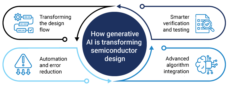
How generative AI is transforming semiconductor design
Generative AI automates the most time-consuming and difficult phases of the process, including floorplanning, placement, and routing. Rather than depending on manual experience and conventional EDA (Electronic Design Automation) tools, generative models learn from enormous amounts of historical design data to propose optimized layouts, forecast potential performance problems, and scale rapidly to respond to new design needs.
This allows faster iteration loops, reduces manual trial-and-error, and reduces design costs significantly. Moreover, AI-powered techniques can optimize multiple goals simultaneously such as power consumption, area utilization, and performance, providing higher quality, smarter designs that are faster to market.
-
Transforming the design flow
Classic chip design is a linear process from idea to finished chip, each stage involving high levels of human intervention and manual optimization. Generative AI is breaking down these barriers by developing smart workflows that automatically adapt and optimize.
In the design phase where high-level ideas are translated into real circuit designs, artificial intelligence chip design software now analyze thousands of past successful designs to find the most optimal routes. Rather than having engineers make manual adjustments on each logic gate, AI can compare millions of configurations at once and pick the best arrangement for performance, power usage, and area utilization.
This transformation becomes stronger in the place and route phase, where billions of pieces must be placed and routed on the chip. Conventional approaches tend to take several iterations and weeks of fine-tuning. AI for chip design addresses this problem by treating it as a difficult optimization problem and weighing area limits, power needs, and timing constraints, all at once to look for solutions human designers may never find.
-
Smarter verification and testing
One of the most significant advances in chip verification is the process of ensuring designs will function properly before costly manufacturing starts. AI within the semiconductor industry is bringing pattern recognition abilities that can detect probable issues much earlier in the design process.
These AI tools learn from massive databases of past chip designs, including both successful and failed prototypes. As they evaluate a new design, they can detect subtle patterns that might indicate future reliability issues, timing problems, or manufacturing issues. The ability to detect such potential problems early reduces expensive redesigns and time from initial idea to product that is ready for market.
Artificial intelligence-driven simulation tools are also minimizing the gap between theoretical design and actual performance. By learning from large databases of real chip behavior, these tools make better predictions about how designs will perform under varying conditions of operation, minimizing the usual disparity between simulated performance and real-world outcomes.
-
Advanced algorithm integration
The most exciting development arises from the incorporation of neural networks and genetic algorithms into the design process. Neural networks, based on the way in which the human brain works, are particularly good at detecting subtle patterns in chip layouts and suggesting original solutions that conventional rule-based systems may not catch.
Genetic algorithms operate alongside these neural networks, effectively “evolving” chip designs over multiple generations of refinement. As with natural evolution, the algorithms begin with simple design ideas and repeatedly refine them, retaining the most effective elements and eliminating less efficient ones.
-
Automation and error reduction
The most realistic advantage of generative AI for chip design is the significant reduction in time spent on manual, repetitive work. Layout generation, which required months of labor from various engineers to achieve, can now be mostly automated to generate the same or even higher-quality outputs.
This automation reduces the process time and human error. AI systems can function round the clock. They never overlook details due to lack of time and focus on quality throughout the design process. Consequently, chips are more uniform, with fewer manufacturing errors and better overall performance.
The process extends beyond technical enhancement. Engineering teams can direct their experience towards innovation and solving problems instead of wasting time on mundane optimization tasks. New engineers can become productive much quicker, as AI tools handle the complexity that previously took years of experience to manage.
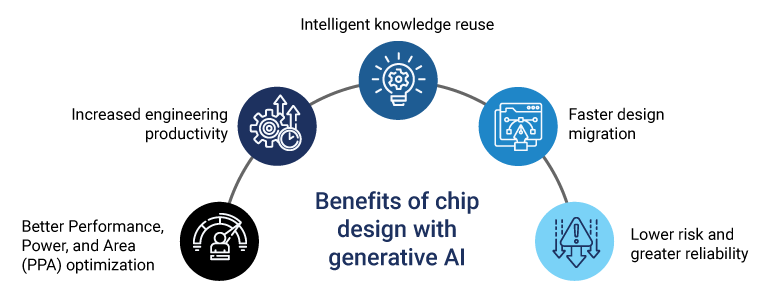
Top 5 benefits of chip design with generative AI
Generative AI in chip design provides powerful benefits that revolutionize both engineering workflows and business results. Below are the prime advantages leading to extensive adoption throughout the semiconductor ecosystem.
-
Better Performance, Power, and Area (PPA) optimization
Traditional chip design limits engineers to exploring hundreds or thousands of design configurations, barely scratching the surface of what’s possible. The use of artificial intelligence for chip designing changes this by evaluating millions of variations simultaneously, often achieving 10-30% performance improvements over conventional methods.
AI systems excel at making hard trade-offs between chip size, power usage, and performance. Human designers may optimize one of these and unintentionally compromise the others, whereas AI for chip design discovers the best overall configurations for applications.
-
Increased engineering productivity
Designers face growing design complexity and diminishing resources. Generative AI applied to chip design handles tedious tasks such as layout optimization, timing closure, and design rule checking. All these activities took weeks earlier but now can be done within a few hours or days.
This increase in productivity enables engineers to work on innovation and problem-solving, saving them time from repetitive optimization activities. This translates to quicker project completion as design cycles come down from 12-18 months to 8-12 months with improved results.
-
Intelligent knowledge reuse
AI within the semiconductor field constructs holistic knowledge bases from each project, with instant access to the insights of hundreds of prior designs. In contrast to conventional methods where knowledge might be lost when engineers retire, AI systems store institutional know-how indefinitely.
This learning capability improves with each project. Businesses employing AI for chip design effectively create smarter tools that improve over time, with every design build on the experience gathered.
-
Faster design migration
As manufacturing processes progress from 7nm to 5nm to 3nm and beyond, AI tools excel at porting designs to next process nodes. This process used to take months of tedious rework before, but now it can be done in weeks, enabling companies to realize new manufacturing technologies rapidly for competitive gain.
-
Lower risk and greater reliability
Artificial intelligence systems forecast potential manufacturing problems and point out design flaws prior to fabrication, avoiding silicon respins that are costly. The constant quality focus that artificial intelligence chip design offers minimizes flaws that can affect product dependability, making a feedback loop of ongoing improvement with every project.
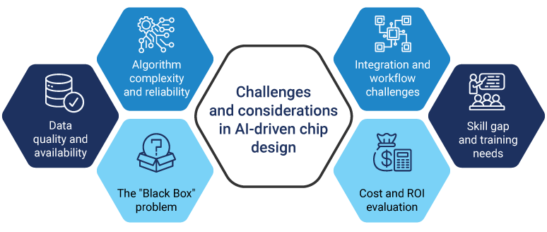
Challenges and considerations in AI-driven chip design
While generative AI in chip design offers tremendous benefits, successful implementation requires careful planning and realistic expectations. Here are the key challenges and considerations for organizations adopting this technology.
-
Data quality and availability
AI algorithms require large amounts of high-quality historical chip design data to train well. However, design data is commonly considered confidential IP, distributed across various teams, or held in incompatible data formats. Inadequate or incorrect data can result in biased models and poor design recommendations.
Key considerations: Review current design data and set standards for collection early. Collaborate with EDA vendors for industry datasets and invest in data preparation processes prior to anticipating best AI outcomes.
-
Algorithm complexity and reliability
It is difficult to build AI algorithms that can manage varied chip design scenarios. Artificial intelligence chip design platforms need to learn to accommodate numerous variations in performance expectations and manufacturing limitations. Algorithms can be inaccurate when encountering design complexities not represented in training data.
Key considerations: Begin with limited, well-characterized use cases and then move to more intricate situations. Create validation procedures and keep human intervention in charge of key decisions until the dependability of AI is established.
-
The black box problem
AI systems tend to be “black boxes,” making it difficult to understand their decision-making processes. This lack of interpretability is not favorable for the industry as it relies heavily on comprehension of design rationale for validation and regulatory compliance.
Key considerations: Select AI tools that are explainable to some extent. Adopt gradual deployment with rigorous validation against conventional methods and consider maintaining parallel design tracks initially.
-
Integration and workflow challenges
Seamless integration of AI for chip design into current EDA tools and processes may be disruptive and difficult. Differences in data formats, compatibility problems, and change aversion can slow the adoption process and reduce the effectiveness of AI.
Key considerations: Implement phased integration. Integrate AI solutions that work in parallel with current processes first and invest in thorough training and change management programs.
-
Skill gap and training needs
Effective AI deployment in the semiconductor sector demands new abilities that merge established industry expertise with AI knowledge. Staff must be trained to work with AI tools, understand output, and recognize when to rely on suggestions.
Key considerations: Build detailed training programs addressing both AI strengths and weaknesses. Establish internal champions to identify value and explore partnerships for semiconductor-focused AI training.
-
Cost and ROI evaluation
AI deployment requires substantial upfront investment in software, training, and possible productivity disruption. Return on investment may be difficult to quantify in short time because many advantages, such as better design quality will not necessarily appear in quantifiable figures immediately.
Key considerations: Begin with pilot programs with definite, measurable value. Set baseline measures prior to implementation and include both direct (shorter cycles) and indirect (fewer respins, higher satisfaction) benefits in calculating ROI.
Future of generative AI in the semiconductor industry
Generative AI for chip design will become as fundamental to semiconductor development as design automation tools are now, revolutionizing the entire industry within the next decade.

-
Expanding applications and capabilities
Artificial intelligence for chip design will extend beyond existing activities such as layout optimization to support entire design flows – from initial architecture to manufacturing. Next-generation systems will support intricate multi-die architectures, sophisticated packaging, and heterogeneous compute platforms and automatically generate design documentation, compliance checks, and patent examination.
Artificial intelligence-based chip design will optimize overall system-level interactions and not just individual pieces, making integration seamless between hardware, software, and applications working together.
-
Solving workforce and sustainability issues
The critical shortage of talent in the semiconductor industry will be addressed as AI systems act as smart mentors, capturing the knowledge from retiring experts and allowing smaller organizations to compete without huge specialist teams.
AI tools of the future will be energy-efficient, optimizing chips automatically for minimum power usage while knowing the full energy life cycle from manufacturing to disposal. This solves increased concerns regarding the environmental footprint of computing infrastructure.
-
Self-improving systems and new markets
The most exciting development will be AI systems that learn from every design project continually, generating feedback loops where implemented chips provide performance data that enhances subsequent designs. Real-world learning will produce advanced capabilities impossible for conventional simulation to deliver.
AI in the semiconductor industry will venture into quantum computing processors, neuromorphic structures, and extreme environment use. Rapid tailoring will make dedicated processors financially viable for specialized use cases, revolutionizing numerous sectors.
-
Timeline and strategic implications
Although fundamental applications exist today, complete transformation will take place over the coming decade with major improvements every two to three years. Early adopters implementing AI tools today will be in the best position to capitalize on future developments and continue to hold competitive advantages.
The alignment of evolving AI capabilities, increasing design complexity, and sustainability needs provides the perfect scenario for accelerated adoption. Businesses that invest in AI talent today will define semiconductor innovation tomorrow, developing solutions that are inherently smarter, more sustainable, and more affordable than ever.
Transform your chip design process
The next wave of semiconductor breakthroughs will be shaped by those who embrace generative AI in chip design early. By adopting artificial intelligence powered chip design tools, businesses can unlock faster development, achieve cost savings, and gain a competitive advantage in a market that waits for no one.
- Google has invented AI that reduced chip placement time from weeks to under 24 hours, outperforming expert designs in power, performance, and area.
- Cadence used AI to optimize a 5nm chip in 10 days with one engineer, versus several months with a team of ten.
This signifies that as AI in the semiconductor industry evolves, it will not only accelerate chip performance but also spark entirely new possibilities in computing, connectivity, and automation.
Rebuild your approach for chip designing because AI for chip design is not just about efficiency, it’s about staying relevant in a rapidly changing digital world. Organizations that act today will be the ones leading tomorrow’s innovation.
FAQs
1. Which AI technologies power generative design in chip development?
Generative AI in chip design uses machine learning, deep learning, and reinforcement learning models. These technologies help explore design options, optimize circuit layouts, predict performance, and automate testing, making the design process faster and more efficient.
2. What is generative AI system design?
Generative AI system design refers to the use of AI models that can create and optimize entire systems such as chips, circuits, or architectures by generating new design possibilities, simulating outcomes, and suggesting improvements. It helps engineers reduce manual effort and discover innovative designs.
3. How is AI used in chip design?
AI is used in chip design for tasks like automating layout design, improving power and performance efficiency, predicting design flaws, and accelerating verification. It allows engineers to test thousands of design variations quickly and find the best solution with less time and cost.
4. How is AI used in the semiconductor industry?
In the semiconductor industry, AI is applied across the value chain from chip design and wafer inspection to manufacturing and supply chain optimization. AI improves yield rates, detects defects earlier, enhances quality control, and speeds up product development.
5. What is the difference between AI chip and normal chip?
An AI chip is specifically built to handle AI workloads like machine learning and deep learning. It is optimized for parallel processing, faster data handling, and energy efficiency. A normal chip, on the other hand, is designed for general computing tasks and is not specialized for AI operations.