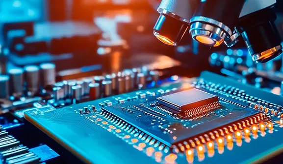
AI-powered wafer defect detection for semiconductor industry
Inspect every wafer in real time with AI to catch defects early and accurately
Talk to an AI expertInspect every wafer in real time with AI to catch defects early and accurately
Talk to an AI expertOur Clients
Traditional visual checks and fixed rule sets struggle as designs get denser and lines run faster. The result is:
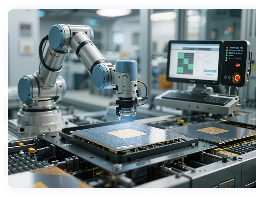
We deliver AI-powered wafer defect detection, from the first dataset to on-tool models that flag issues early and drive measurable yield gains.

We capture your data, label real defects, and train on your specific defect types. Our models then run on the tool with expert review. The output feeds Statistical Process Control (SPC), while confirmed labels build the retraining set. Thus, accuracy and speed improve with each batch.

We combine confocal and structured illumination streams with 2D images when depth is needed. This combined view of image and height data improves decisions on surface recess after Chemical Mechanical Planarization (CMP), erosion, voids, and contact heigh variation.

Operators, engineers, and QA get role-based views with live flags, defect maps, and batch analytics. Secure APIs sync results with Manufacturing Execution Systems (MES), SPC, and your data platform, so actions and ownership stay clear.
See how our solution fits your tools, systems, and workflows.
Book a callOur AI inspection improves accuracy, speeds decisions on the line, and turns findings into actions that show up in your yield.

Flag defects early with consistent calls across tools and shifts. Since the models learn subtle patterns and micro-defects that manual checks miss, the review workload stays manageable.

Performance improves over time rather than stalling after go-live. As products, layers, and tools evolve, models learn from new labels and live production data without major rule changes.

Reduce false alarms to reduce unnecessary line stoppages. More reliable classification separates critical from non-critical defects, which keeps engineers focused on the work that matters.

Keep inspection at line speed rather than slowing the station. With real-time inference and a streamlined review queue, rechecks drop, disposition moves faster, and cycle time shortens.

Improve first-pass yield while keeping output stable. Because earlier detection lowers scrap and stops defects from reaching later steps, flow across the line stays steady.
Automatic Defect Classification (ADC)
Classify defects fast with clear severity
Real-time analysis for inline feedback
Flag defects on the line for quicker action
Anomaly detection for new or rare defects
Detect outliers using few samples
Integration with factory systems
Sync with MES and SPC for closed loop audit
Explainable AI and visualizations
Act faster with overlays and heatmaps

Combine three-dimensional height maps with images to flag topography-linked issues such as surface recess after Chemical Mechanical Planarization (CMP), erosion, voids, and contact height variation. The classifier uses texture and shape together to sharpen precision on challenging cases. By aligning 2D and 3D data in one coordinate system, engineers review once with the right evidence in view. Results then link to factory systems for traceable actions and continuous improvement.

Pair high-resolution camera data with AI models to detect particles, scratches, shorts, and pattern breaks. Lightweight setup and standard templates bring new products and batches online faster, while recipe changes stay simple to manage. Because detection is consistent across tools and shifts, review time is more predictable, and engineers can focus on high priority tasks.

Align images and measurements to the same coordinates, so each defect links to its exact measurement point. This single-view workflow helps process, yield, and quality assurance (QA) decide next steps without back-and-forth. With fewer handoffs and clearer evidence, reviews shorten, and corrective actions move sooner.

Connect scanning, inference, and action into one high-throughput flow that matches production speed. Built-in review queues and auto-rules close the gap between detection and decision, keeping each stage connected and responsive. As line conditions change, the system maintains pace, keeping inspection aligned with production targets and sustaining throughput.
Boost yield and minimize losses with AI-powered wafer inspection
Request a demo nowIndustry
Semiconductor
Technologies
Python, TensorFlow, Keras, Azure Blob Storage
Challenges
Business impact
Client
A large-scale manufacturer of semiconductors
Industry
Semiconductor
Technologies
AI, ML, Deep learning, TensorFlow, PyTorch, and Python
Challenges
Business impact
Client
A semiconductor manufacturer
Bring AI wafer inspection to your line
Share your setup and goals, and we’ll map a tailored plan with clear next steps and measurable targets.
 100% Secure. Zero Spam.
By submitting this form you agree with the terms and privacy policy of Softweb Solutions Inc.


