How Softweb achieved 94.3% defect detection accuracy for a global semiconductor manufacturer using AI-enabled inspection
Our client is a global semiconductor manufacturer supplying chips and electronic components to OEMs and electronics companies across multiple industries. They partnered with Softweb to strengthen inspection accuracy and reduce dependency on manual review through an AI-driven defect detection approach.
 Industry: Semiconductor manufacturing
  Business type: Enterprise
  Services: AI-based defect detection solution
  Technology:AI, ML, Deep learning, TensorFlow, PyTorch, Python
Client profile
Our client operates in semiconductor manufacturing, producing chips used across automotive systems, consumer electronics, and communication networks. With a global customer base and operations spanning multiple regions, their production environment depends on precision, consistency, and process reliability at scale.
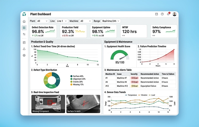
Their inspection workflows span multiple stages, where each layer of wafer processing must be validated before moving forward. Maintaining consistency across these stages is critical to ensuring overall product quality and yield performance.
Technical challenges
The client’s inspection processes relied on a mix of manual review and traditional vision systems. While these methods supported baseline quality checks, they struggled to keep pace with increasing complexity and production scale.
Manual inspection limits
Manual checks were time-intensive and inconsistent, making it difficult to detect micro-level defects reliably at scale.
Rule-based vision gaps
Complex and evolving defect patterns pushed traditional systems beyond their detection limits, with accuracy declining over time.
Layered inspection risks
When defects in early wafer layers went undetected, they propagated forward and raised both rework volumes and yield loss.
Data labeling delays
Large volumes of labeled image data took significant time to prepare, which pushed back model training timelines.
Our solution
We designed and implemented an AI-driven defect detection solution that combined machine learning, deep learning, and computer vision within the client’s inspection environment. The approach was aligned with their existing workflows so that improvements could be introduced without disrupting ongoing operations.

We focused on making the data usable, aligning models with actual inspection conditions, and connecting outputs back into production systems. The setup ensured that inspection outputs could be used directly within the workflow, without adding delays or manual dependency.
Structured data collection and preprocessing for model readiness
We gathered and organized data from multiple sources within the manufacturing environment, including defect logs, production parameters, equipment performance metrics, and maintenance records. Each dataset was cleaned and aligned so the models could work with consistent inputs across different inspection scenarios.
As the data became more consistent, the models began to respond more reliably. Noise reduced, patterns became clearer, and detection results improved with each iteration. The same structure also made it easier to update models without rebuilding the pipeline.
Applying machine learning and deep learning techniques for defect detection
The inspection workflow worked with both structured datasets and image-based inputs, so each required a different way to interpret the data. We used decision trees and random forests to process structured inputs, while convolutional neural networks handled defect detection within inspection images.
These models worked together to improve detection coverage across inspection stages. They identified visible defects with greater precision and helped uncover patterns that were not immediately apparent. The team tuned the models to maintain stability across varying inspection conditions.
Training and validating models using scalable deep learning frameworks
We built and trained models using frameworks such as TensorFlow and PyTorch, following a structured development process. Data was split into training, validation, and testing sets to ensure models could generalize effectively across unseen data.
Validation and parameter tuning continued throughout development as new data was introduced. Adjustments were made based on how the models responded under different conditions, which helped maintain reliability without performance drift.
Integrating AI models into semiconductor inspection workflows
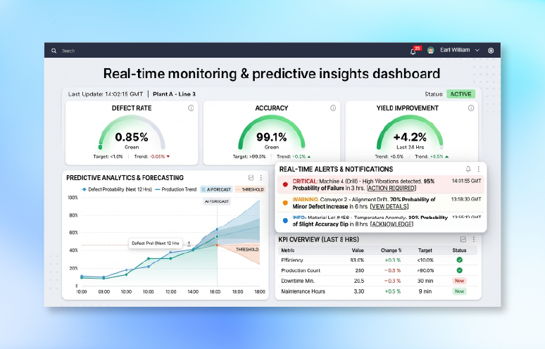
We integrated the trained models into the client’s existing manufacturing systems to enable real-time inspection and decision-making. The solution supports continuous data ingestion, model inference, and automated feedback into control systems.
Dependency on manual checks reduced, and inspection results became available directly within production workflows. Teams responded faster to defects while maintaining process continuity across inspection stages.
Business goals and measurable outcomes
| Business objective | Business benefit delivered |
|---|---|
| Improve defect detection accuracy | Achieved 94.3% detection accuracy, improving consistency across wafer inspection stages |
| Reduce manual inspection effort | Automated inspection reduced reliance on manual checks while maintaining consistent output |
| Enable faster defect identification | Real-time detection helped teams identify and address defects earlier in the process |
| Strengthen production efficiency | Streamlined inspection workflows reduced delays and supported stable throughput |
| Support scalable inspection systems | The solution handled increased volumes without impacting inspection speed or accuracy |
Tech stack
- Programming & Frameworks:
- Python, TensorFlow, Keras
- AI/ML Techniques:
- Machine Learning, Deep Learning, Computer Vision, Convolutional Neural Networks (CNN)
- Data Processing:
- Data Preprocessing, Feature Engineering, Data Labeling & Validation
- Modeling Techniques:
- Decision Trees, Random Forest, Transfer Learning
- Deployment & Integration:
- Real-Time Model Inference, API-Based Integration with Inspection Systems
- Architecture:
- AI-Powered Defect Detection Pipeline for Semiconductor Inspection
- Platform Capability:
- Scalable AI Models for High-Volume Manufacturing Environments
Similar case studies
Enhanced quality control system for a manufacturing company with machine learning
Automatic defect detection on semiconductor wafer surfaces using deep learning
Ensuring high quality packaging with computer vision
Connect Now
Our experts would be eager to hear you.
