Share
Share
 ChatGPT
 Perplexity
 Claude
 Grok
Grok
 Google AI Mode
A single 300mm wafer at an advanced node now costs a fab somewhere between $16,000 and $22,000 to process. That cost is fixed the moment the wafer enters the line. What is not fixed is how many of the chips stamped onto that wafer actually work. And that one variable, yield, is the difference between a healthy margin and a business case that never closes.
At the volumes leading foundries run, for example, Taiwan Semiconductor Manufacturing Company (TSMC) alone manufactured over 17 million 12-inch equivalent wafers in 2025. At this scale, a 1% yield improvement on a single product line can mean millions of dollars in extra revenue. That’s why data, artificial intelligence (AI), and machine learning (ML) have moved from “innovation lab” projects to core production infrastructure running inside the world’s largest fabs today. Here’s how it helps them.
How Data, AI, and ML optimize wafer economics
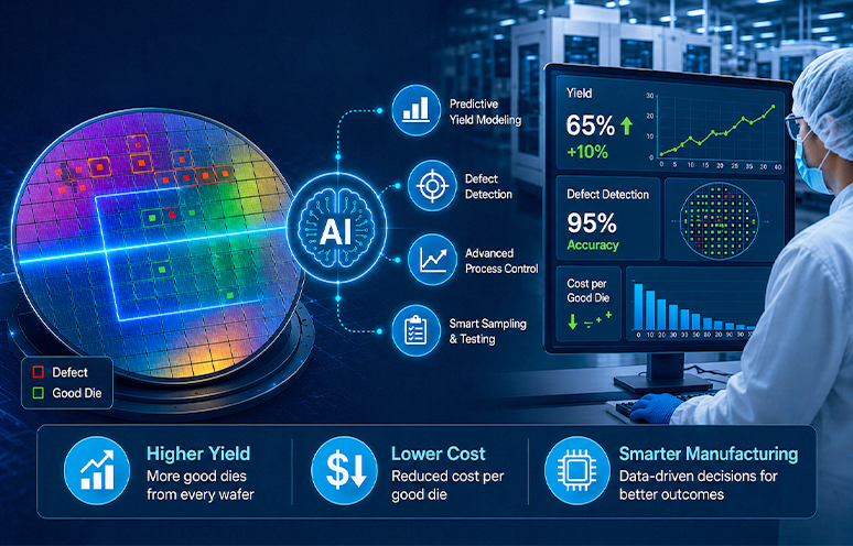
1. Predictive yield modeling: Rather than waiting for the final electrical test to learn whether a wafer succeeded, ML models can estimate the probability of failure at intermediate process steps. These models are trained on historical wafer maps, defect logs, and parametric test data. Catching a doomed wafer early means the fab can stop pouring additional processing costs into it. It can also redirect fab capacity or adjust downstream recipes before the defect propagates to the rest of the lot.
2. Automated defect classification (ADC): Deep learning and convolutional neural networks now perform the visual inspection work that used to fall to human operators. These operators used to review images from optical and e-beam scanners by hand. Modern wafer-inspection systems use deep learning to detect and classify defects automatically, often as well as or better than human inspectors. And because the models run continuously instead of on a sampled basis, defects show up in near real time instead of during the next business day’s review.
3. Advanced process control (APC): There are physical variables, like etch rate, chamber temperature, and deposition pressure, that decide whether a die comes out functional. On real tools, they drift constantly. The time a process step actually needs can also change from wafer to wafer. So, a fixed recipe timing can let a process run too long, past the point where it produced the best result, wasting material or damaging the chip. By feeding live tool-sensor and metrology data into machine learning models, fabs can capture the nonlinear relationships between process time and outcomes. This lets them set optimal process times per wafer or per batch, tightening the process window instead of just monitoring it after the fact.
4. Adaptive sampling and testing: Testing every die at every step is too slow and expensive at advanced-node volumes. So, AI-driven sampling strategies instead point out the fab’s limited testing bandwidth at the wafers and dies that historical pattern flag as higher-risk. Lower-risk lots move through with lighter-touch inspection instead. This recovers cycle time without giving up coverage where it matters.
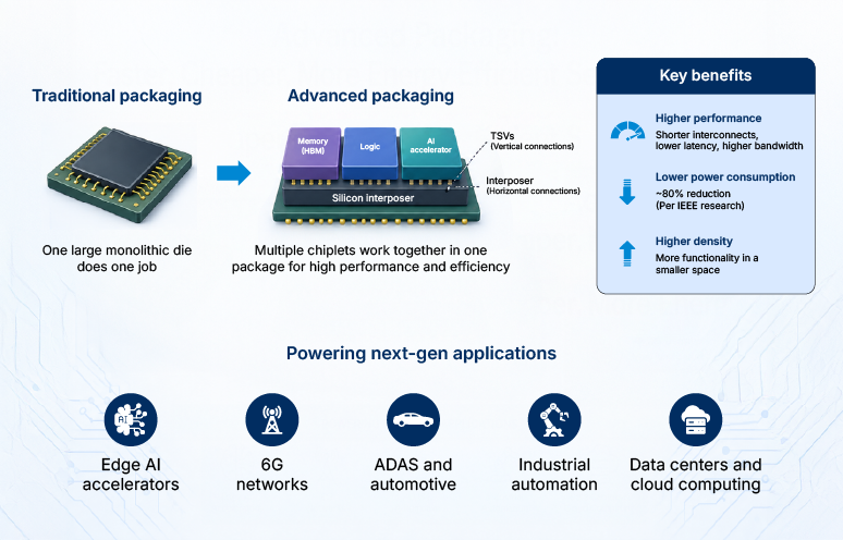
5. Chiplet and die-to-die architecture: As monolithic dies for large AI accelerators grow, their defect exposure grows with them. A bigger die simply has more silicon area where a single particle can kill the whole chip. The industry’s response has been to break large designs into smaller chiplets instead. Each chiplet is fabricated, tested, and confirmed good before it’s bonded together with others in advanced packaging.
ML tools play a growing role here too. They help manage the enormous test and pairing data needed to match known-good chiplets, and they help predict the structural reliability of the resulting heterogeneous package. In effect, this moves part of the yield equation from “can we make this whole die work” to “can we assemble enough working pieces.”
Taken together, these levers attack the yield equation from every angle.
- Fewer wafers get processed to a dead end
- Defect detection is faster and more accurate
- Process control is tighter
- Test resources are allocated more smartly
- The architectures become yield tolerant by design
How die-per-wafer economics decides the payout of every yield gain in semiconductor manufacturing
Every die-per-wafer conversation starts with gross die vs. net good die from a wafer. Gross die count is the maximum theoretical number of dies that could physically fit on a wafer. What a fab ships and gets paid for is the net good die count. It is gross dies minus everything lost to particle contamination, lithography defects, etch and doping variation, and packaging stress.
Math is simple. The cost per good die = wafer processing cost ÷ net good dies. Here’s how that shifts as yield moves, on a $18,000 processing cost, 600-gross-die wafer at a 55% baseline yield.
| Yield scenario | Net good dies (of 600 gross) | Cost per wafer | Cost per good die | Saved per good die (vs. baseline) |
|---|---|---|---|---|
| Baseline yield (55%) | 330 | $18,000 | $54.55 | — |
| +3 points (58%) | 348 | $18,000 | $51.72 | $2.82 |
| +10 points (65%) | 390 | $18,000 | $46.15 | $8.39 |
If we add saved per good die cost to TSMC’s 17M figure, the company can save $1.32 billion and $3.92 billion monthly with 3% and 10% yield improvement, respectively.
New process nodes make this harder before they make it easier. A 3nm or 5nm line typically ramps from initial yields of 50-60% toward maturity over months, and the steepness of that ramp determines whether a new node is profitable on schedule. The traditional way of climbing that curve, a senior engineer manually inspecting wafer maps and cross-referencing tool logs, works on mature nodes. It breaks down at the leading edge, where defect signatures are subtler and a single fab can generate 5 to 20 terabytes of process and inspection data per day. Data, AI, and ML don’t replace the yield engineer’s judgment; they compress the search space so that judgment gets applied to the right ten wafers.
What target state a fab can achieve with data, AI, and ML
In an ideal future state, a fab’s yield management is powered by AI. The system continuously ingests inspection images, metrology data, live sensor streams, and everything else engineers use for defect detection as explained through the above image. ML models classify known defect patterns and flag new, unusual issues for review. By connecting defect signatures with upstream process parameters, these models can suggest likely root causes within hours. Speed is the entire point here, since faster diagnosis means fewer wafers processed toward eventual scrap.
With data analytics in semiconductor setup, yield engineers spend less time on manual data scanning and more time reviewing AI-generated insights. They make decisions on hold lots, qualify process changes, and remain the final authority on every action. Each decision made by a human is fed back into the AI system. It improves its accuracy over time. Engineers are still in control. They just get better and faster guidance from AI, making the entire process more efficient and effective.
The following matrix defines the measurable operational boundaries that differentiate a manually sampled fab from a fully AI-integrated manufacturing facility.
| Metric | Manual/Baseline state | AI-driven target state |
|---|---|---|
| Defect classification accuracy | 70% – 80% accuracy, heavily bottlenecked by manual inspection of sampled lot subsets. | ≥ 95% accuracy applied uniformly across 100% full wafer coverage. |
| Excursion response window | Root cause analysis drags on for 2 to 5 days, which risks massive inline contamination. | Confirmed root cause compression down to a tight 4 to 12 hours. |
| Yield improvement at advanced nodes | Standard yield learning curves during new node introductions. | 5-10% higher yield during the critical ramp phase. |
| Scrap wafers per excursion event | Excursion events routinely ruin thousands of wafers before the line is halted. | Content containment limits damage to just hundreds of wafers per event. |
Source: Metrics compiled from foundry and Integrated Device Manufacturer (IDM) deployment patterns.
Two of these rows are worth dwelling on. The jump from days to hours in root-cause analysis matters because every hour of delay lets more wafers move through a process that’s already producing bad die. That delay compounds the cost of the defect with each passing hour. The fix arrives too late to help the wafers already in flight. And the shift from “thousands of scrap wafers” to “hundreds” per excursion event is, in dollar terms, the difference between a bad and excellent quarter, at $16,000-$22,000 a wafer.
How has AI performed in production for global scale semiconductor manufacturing companies
The industry’s biggest names are already running AI in production at full fab scale, with numbers to prove it.
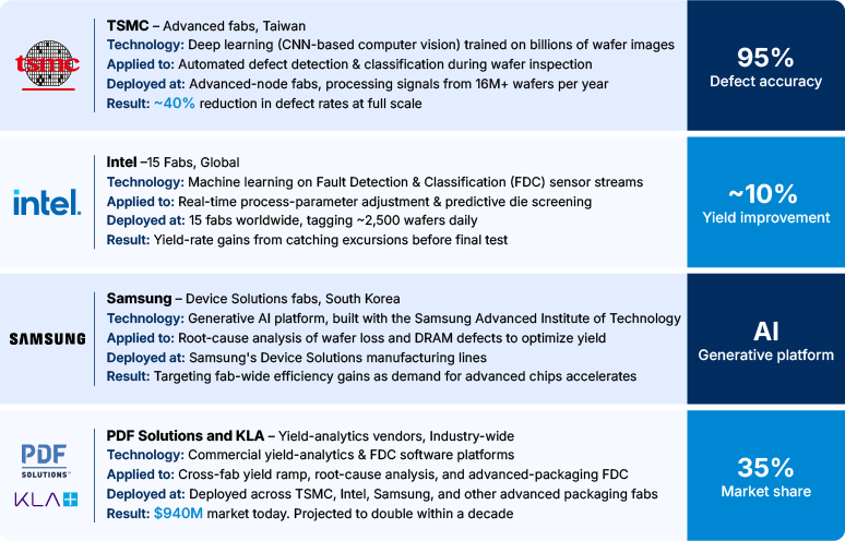
Where the value lands when implementing AI in semiconductor manufacturing
It’s worth being precise about where this value shows up on a semiconductor company’s books. It goes to cost, not top-line growth.
Industry research frames it explicitly. Across the value chain, manufacturing captures the most value from AI and machine learning. These use cases reduce costs, improve yields, and increase fab throughput. And over the long run, they’re projected to cut manufacturing costs (both COGS and depreciation), sometimes by up to 20%.
Every good die recovered from an already paid for wafer is an incremental margin. Companies can sell such good dies at full price with zero additional capital spent to produce them.
Our four recommendations to help you capture the yield value using data, AI, or ML
Capturing yield or cost value is not just a modeling exercise. It requires designing around constraints most enterprise AI use cases never face.
- Keep data on-prem. Process data is highly proprietary. Run models on-premises or in air-gapped environments, so no data leaves the foundry.
- Integrate deeply, don’t bolt on. Build ecosystems that plug into your existing MES, FDC, and yield management systems already running the fab.
- Design for speed. The line runs 24/7. Keep inference latency under minutes per wafer lot and make sure retraining never disrupts production data pipelines.
- Keep humans in the loop. Use AI to surface hypotheses and flag anomalies. But let the engineers make the final call. That means decisions like pausing a batch of wafers for inspection, adjusting the recipe, or approving a new process to go live. Their dispositions become training data. Over time, this feedback loop is what makes the AI smarter.
The bottom line: One fraction decides everything
Die-per-wafer economics reduces to one relentless equation: Fixed wafer cost ÷ Variable good-die count.
Every AI and ML investment a fab makes is ultimately an attempt to grow the denominator without touching the numerator. That includes:
- Predictive yield models
- Automated defect classification
- Advanced process control
- Adaptive sampling
- Chiplet architectures
At $16,000 to $22,000 per wafer, and tens of thousands of wafers start a month, a few percentage points of improvement compound fast. Fabs that get better at this one fraction are unlocking tens of millions of dollars in revenue that was already sitting on the line.