Share
Share
 ChatGPT
 Perplexity
 Claude
 Grok
Grok
 Google AI Mode
In 1965, Gordon Moore stated that the number of transistors on an integrated circuit (IC) doubles approximately every two years. For years, semiconductor manufacturers have associated performance gains with shrinking transistor sizes, as it has driven the Power, Performance, Area, and Cost (PPAC) framework. But today, transistors have shrunk to atomic sizes. Such a scale causes quantum tunneling and generates massive heat.
Therefore, instead of miniaturizing chips, engineers combine multiple chips into a single integrated system using advanced packaging techniques. Traditionally, a conventional chip does one job. An advanced multichip package performs many functions by bringing memory, logic, and specialized silicon together into a single component. It solves the semiconductor industry’s toughest challenges, from higher processing speeds and lower manufacturing costs to better power efficiency.
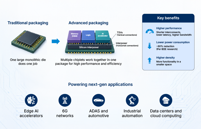
Advanced packaging helps semiconductor manufacturers, like logic and memory Integrated Device Manufacturers (IDMs) and foundries with leading node capabilities to meet the demand of their customers. These end customers are data center providers, automotive OEMs, home appliance manufacturers, and computing device makers. They need semiconductors that run emerging applications like edge AI accelerators, 6G, ADAS, industrial automation, and so on. These applications require high-performance and low-power chips that can quickly process massive quantities of data.
Since advanced packaging offers a higher-value opportunity, it attracts major players like Intel, Texas Instruments, Samsung, SK Hynix, and fast followers (organizations that imitate competitors’ innovations) to win premium customers. In this blog post, we describe how advanced packaging can help you build semiconductors that are faster, cheaper, and more energy efficient.
What is advanced packaging?
Advanced packaging is the suite of techniques that combine multiple silicon dies (chiplets), such as Logic, High-Bandwidth Memory (HBM) stack, and AI accelerator, within a single physical package. It allows them to function as a unified chip.
Traditionally, Outsourced Semiconductor Assembly and Test companies (OSATs), foundries, and Integrated Device Manufacturers (IDMs) design and manufacture one large monolithic die. They then attach it to a substrate using wire-bonding or flip-chip technologies. This miniaturization approach worked well when 40nm nodes were mainstream in 2008-09. Today, Taiwan Semiconductor Manufacturing Company (TSMC) and Intel aim for mass production of 1nm nodes by 2029. At this scale, advanced packaging offers a promising way to sustain the PPAC framework.
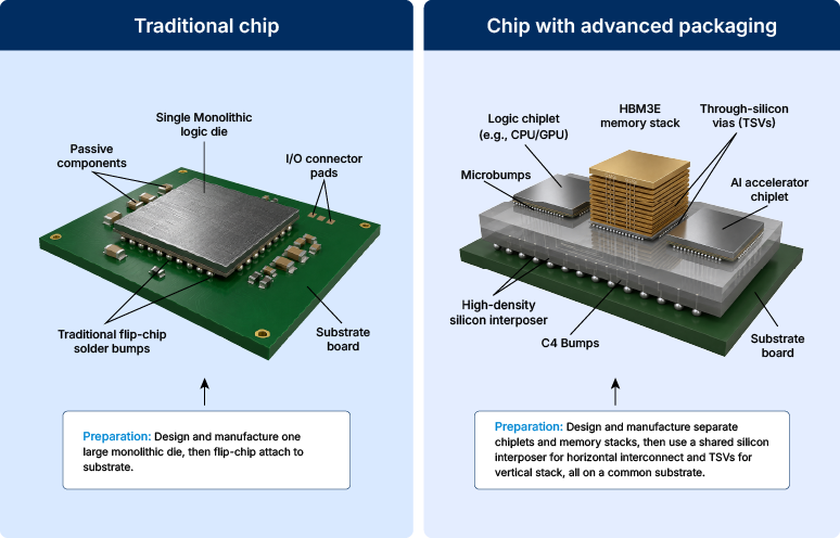
In advanced packaging, these players design and manufacture separate chiplets and memory stacks instead of one large die. They connect these components using:
- A shared silicon interposer for horizontal links
- Through-Silicon Vias (TSVs) for vertical stacking
Semiconductor manufacturers then attach these connected components to a common substrate.
Ingredients like TSVs offer:
| Benefit | Impact |
|---|---|
| Better electrical performance | Improved signal integrity and connectivity |
| Lower power consumption | ~80% reduction (per research published in IEEE) |
| Greater data width and bandwidth | Stronger throughput between components |
| Higher density | Increased component density per package |
These gains in performance, power, and density deliver measurable advantages. The sections below walk you through how these building blocks drive speed, cost savings, and efficiency across the packaging process.
How advanced packaging accelerates performance
Monolithic dies put every function onto one substrate, which limits how fast signals travel. Advanced packaging shortens interconnect distances by placing chiplets closer together on a shared interposer. Shorter distances mean signals face less resistance and reach their destination faster.
TSVs create vertical pathways that let logic and memory stacks communicate directly. Such high-density interconnects reduce the physical distance data has to travel between dies. The following 3D diagrams highlight the key advanced packaging techniques, 2.5D, 3D, FOWLP, and Co-Packaged Optics, that drive this low-latency performance.
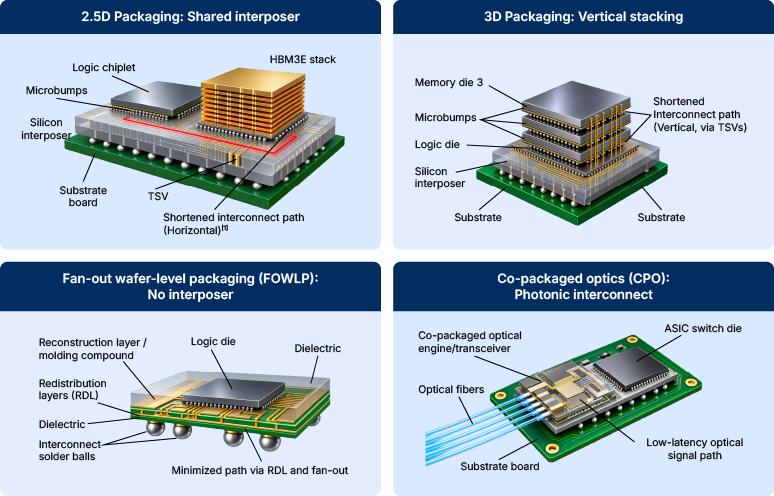
Such vertical stacking cuts the physical distance data has to travel between dies. These arrangements give IDMs and foundries the ability to offer customers higher bandwidth for demanding workloads like data center servers.
Here are a few applications where the speed advantage matters.
- Edge AI accelerators: They process massive datasets locally without relying on constant cloud connectivity. Advanced packaging gives logic and HBM stacks the proximity required for real-time inference.
- 6G infrastructure: It requires the capability of processing enormous data volumes with near-zero latency tolerance.
- ADAS systems (automotive OEM vehicles): Also depend on near-zero latency. To meet strict latency needs, manufacturers use silicon interposers to connect components packed tightly together using advanced packaging techniques.
Instead of printing an entire chip on a single piece of expensive silicon, designers build modular chiplets for each component. For example, high-speed logic is printed on cutting-edge nodes while memory uses mature and cost-effective nodes. Designers join them via advanced packaging techniques. Such heterogeneous integration boosts speed and lowers costs.
Chipmakers reduce manufacturing costs by adopting advanced packaging
Shrinking transistors toward 1nm nodes demands precise lithography and exotic materials. Every additional nanometer of miniaturization multiplies fabrication complexity and drives yield rates downward. Advanced packaging offers OSATs and foundries a way to avoid these escalating costs.
Using advanced packaging, manufacturers can save costs with:
- Higher yields: Smaller chiplets carry a much lower probability of containing a major defect. Fewer defects mean less wasted dies and reduced production expenses.
- Targeted rework: When a defect appears, only the affected chiplet needs replacement or rework. Monolithic dies, by contrast, force manufacturers to scrap the entire chip.
- Reusability across products: Fast followers benefit since chiplets can be reused across product lines. A single AI accelerator chiplet might serve data center, automotive, and computing device customers alike, spreading design and validation costs across multiple revenue streams.
- Selective node allocation: Memory stacks like HBM can be manufactured separately from logic on mature nodes. That reduces the need for costly leading-node capacity for every component, helping foundries manage capital expenditure more efficiently across their fabs.
How advanced packaging cuts power consumption
Heat generation becomes a big challenge once transistors approach atomic-scale limits. Quantum tunneling effects at these dimensions cause current leakage and heavy power loss. Advanced packaging addresses this efficiency problem by rethinking how components connect physically.
Shorter interconnects between chiplets mean electrical signals encounter less resistance during transmission. It reduces energy wasted as heat during data transfer. Research published in IEEE points out that manufactures can achieve nearly 80% power consumption reduction through this method.
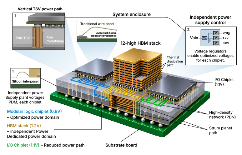
By replacing long PCB traces with ultra-short vertical and horizontal interconnects, advanced packaging minimizes energy wasted as heat. The 3D diagram below illustrates how vertical stacking and independent voltage domains reduce overall power consumption.
Advanced packaging cuts power consumption through three main ways:
- Through-silicon vias: These ingredients replace long horizontal wire bonds with short vertical paths.
- Vertical stacking: By shortening the wiring between layers, this method minimizes unwanted parasitic capacitance, the wasted charge built up along long wires. It results in reduced power loss and improved overall energy efficiency.
- Dedicated chiplets per function: The design approach splits functions into separate chiplets. It allows each component, such as logic, memory, or I/O, to run on its own independent power supply. Instead of forcing the entire chip to run at the high voltage required by the fastest circuits, each chiplet operates at its ideal voltage. Ultimately, this eliminates the power leakage and waste caused by mismatched voltage levels.
Reduced heat and lower power consumption give home appliances and consumer devices a clear edge. For industrial automation, this efficiency is essential to keep systems running 24/7.
These efficiency gains create large datasets that make AI-driven optimization both necessary and possible. As packaging processes scale, this data becomes too complex for manual analysis alone to handle. Over time, this data can become one of the most valuable assets driving smarter design decisions.
How you can use data and Artificial Intelligence (AI) in advanced packaging
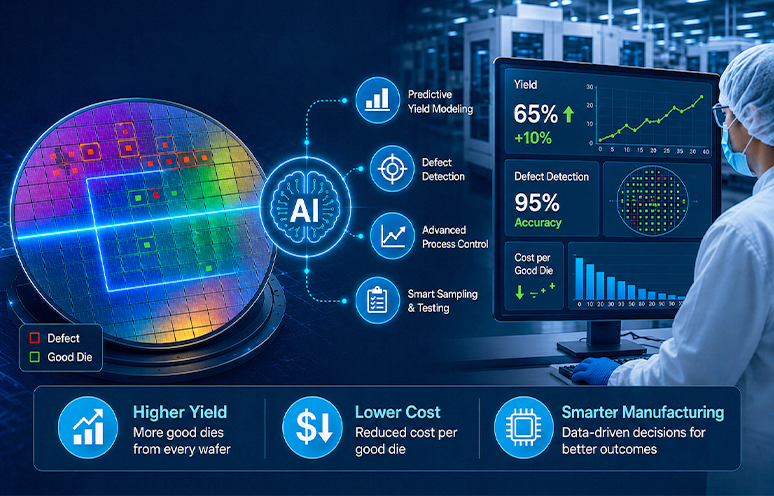
Advanced packaging generates process data in big volume and variety at every stage. This data can become a competitive asset in its own right. By applying AI models, IDMs and foundries can catch packaging issues early. This approach shortens development cycles and eliminates the trial-and-error that traditionally drives packaging costs. As chiplet architectures grow more complex, manual review simply cannot keep pace with the number of variables involved.
| Application area | How AI/Data helps |
|---|---|
| Design and routing | AI optimizes interposer layouts and TSV placement |
| Defect detection | Machine vision models flag micro-defects during die inspection |
| Yield prediction | Predictive models forecast yield loss before packaging begins |
| Thermal management | AI simulations model heat dissipation across chiplet stacks |
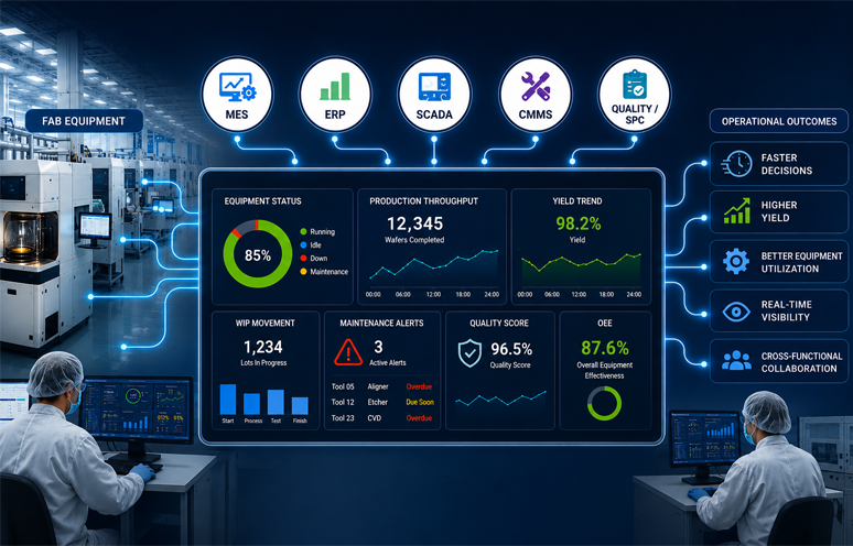
| Increase equipment utilization | More productive tool uptime and stable production flow |
| Supply chain | Data analytics track chiplet inventory and sourcing risk |
On the design side, generative AI tools can simulate thousands of interposer routing and TSV placement variants quickly. It helps engineering teams identify the most efficient layout for signal integrity and thermal performance without running costly physical prototypes. This kind of AI-assisted engineering research is already paying off elsewhere in the semiconductor supply chain. Softweb Solutions built a Databricks-powered engineering intelligence platform for an electronics manufacturer that cut engineering research time by 65% and component evaluation effort by half. This approach applies to chiplet and interposer design work as well.
For example, document intelligence was one of the solutions Softweb Solutions delivered. The solution pulls out technical attributes, operating characteristics, and specifications in seconds. Applied to packaging, that same extraction approach can pull TSV pitch, aspect ratio, keep-out zones, interposer material specifications, and much more from the foundry design rule documents. This will turn a manual specification reading exercise into an instant, searchable reference for engineering teams. Over time, data and AI capabilities will move from high-value design help to standard practice in advanced packaging.
If you want to read more about the role of data and AI in advanced packaging, check out the review paper, ”Advanced semiconductor packaging design via artificial intelligence and machine learning: A review”.
How big is the advanced packaging opportunity?
Analysts expect steady growth across the advanced packaging market. Estimates vary by research firm, but the direction stays the same. Demand from AI, automotive, and data centers keeps pushing numbers upward. The table below summarizes recent projections from a few research firms.
| Source | 2025 market size in billions | Projected size |
|---|---|---|
| Fortune Business Insights (Advanced packaging) | $45.13B | $94.33B by 2034 |
| Precedence Research (Advanced packaging) | $55.2B | $160.1B by 2035 |
| Mordor Intelligence (Advanced packaging) | $51.62B | $90.11B by 2031 |
| Grand View Research (Advanced packaging) | $41.7B | $66.0B by 2033 |
Figures differ by scope and methodology across these reports. Every estimate still points toward strong double-digit growth.
Here are three simple steps for adapting advanced packaging
1. Find where it matters most
Start by looking at your product lineup and ask: which chips are big, complex, and packed with logic? Such logic-heavy chips are the best candidates for applying advanced packaging techniques. This approach helps you find the strongest starting points. For example, situations where speed (low latency) matters, such as in High-Performance Computing (HPC) systems for AI training or scientific simulations.
2. Partner instead of building everything yourself
Advanced packaging requires specialized skills, particularly around interposers and TSVs. Rather than developing all these in-house, consider partnering with OSATs and interposer specialists who already have this expertise.
Some of the established names worth evaluating include:
- ASE Technology and Amkor – the two largest OSATs globally, with deep experience in advanced packaging for AI and HPC applications.
- JCET – a fast-growing player, specifically active in chiplet and heterogeneous integration.
- TSMC – a foundry-side option known for its CoWoS packaging, widely used in AI GPU integration.
- Intel – another foundry-side option, offering Foveros and EMIB packaging technologies.
Each brings different strengths depending on whether you need high-volume packaging, cutting-edge 2.5D/3D integration, or foundry-adjacent services. It’s worth mapping your specific technical requirements, from chip complexity and volume to time-to-market, against what each partner does best before choosing.
These co-development agreements can speed up your time-to-market and spread the financial risk of advanced packaging development.
Packaging partnerships solve the hardware side. But making those components intelligent requires data and AI. By applying predictive analytics, AI-driven quality control, and real-time operational data, you can deliver optimal efficiency and long-term value. That’s where Softweb Solutions comes in, combining data engineering and AI expertise to help you maximize the return on your advanced packaging approach.
3. Design chiplets you can reuse
.
Finally, aim to build chiplets that aren’t just for one product. Build them in a way that you can reuse across markets, from data centers and automotive to consumer electronics. A flexible and modular chiplet toolkit lets you mix and match components for different customers instead of designing it from scratch each time. This positions your company to capture high-value customers as demand grows over the years for edge AI, 6G, and ADAS.