Share
Share

 ChatGPT
 Perplexity
 Claude
 Grok
Grok
 Google AI Mode
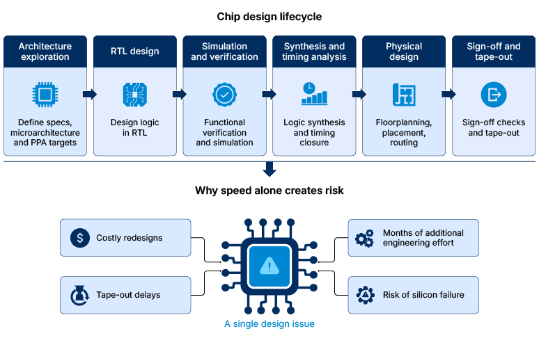
AI-powered digital solutions help semiconductor companies shorten chip design cycles by automating engineering tasks, analyzing design data, and identifying potential issues earlier in the development process. As chip architectures become more complex, even a single design issue discovered during verification can trigger costly redesigns, delay tape-out and consume months of additional engineering effort. The challenge is to achieve this speed while ensuring that every design is accurate, fully verified, and ready for first-pass silicon.
McKinsey estimates that the cost of designing a leading-edge chip has increased from approximately $28 million at the 65 nm node to nearly $540 million at the 5 nm node, making every design iteration significantly more expensive. At the same time, McKinsey estimates that AI and machine learning can reduce semiconductor R&D costs by 28% to 32% by improving efficiency across research, chip design, and verification workflows.
In this blog, we will explore why chip design speed alone cannot guarantee good results, where AI introduces the biggest accuracy risks, and what semiconductor companies can do to move fast without compromising engineering accuracy.
Why are semiconductor companies racing to accelerate chip design?
Semiconductor companies are accelerating chip design to meet growing market demand, shorten time-to-market and stay ahead in an increasingly competitive industry. Increasing demand for AI processors, autonomous vehicles, edge devices, and high-performance computing have shortened product development cycles, leaving no room for delays.
McKinsey states that the ratio of product life cycle to product-development time in semiconductors is half that of a mobile phone, and a third that of an automobile. For the top 20 semiconductor players, R&D costs have continuously risen and now account for more than 20% of revenue.
At the same time, modern chips contain billions of transistors, multiple IP blocks, and complex architectures, making design and verification a resource-intensive process. However, accelerating design speed introduces a new challenge of maintaining engineering accuracy as design cycles continue to shrink.
Why isn’t speed enough in chip design?
AI can shorten chip design cycles, but it cannot eliminate the complexity of engineering decisions. Without rigorous validation and verification, faster design can increase downstream risks instead of reducing time-to-market.
Chip design is a complex process
Modern chips contain billions of transistors. They have multiple IP blocks and heterogeneous architectures that must work flawlessly together. Every component needs to function accurately across millions of operating conditions, making design validation a complex process. For example, Apple’s chips went from 1 billion transistors in 2013 to 20 billion transistors in 2024. AI speeds up individual tasks, but it does not simplify the underlying complexity.
Verification consumes nearly 70% of the chip design cycle
Industry estimates from Synopsys and semiconductor EDA providers indicate that functional verification requires approximately 60%–70% of overall chip development effort. Although AI enhances design speed, engineering teams still need to spend time verifying designs are accurate before tape-out.
Every engineering decision requires balancing power, performance, and area (PPA)
Every design decision affects power, performance, and area (PPA). AI can quickly evaluate trade-offs and suggest options, but engineers must choose the right balance for the product, such as prioritizing battery life in smartphones or performance in data center chips.
A single design issue can trigger rework across multiple downstream stages
Chip development spans RTL design, simulation, verification, synthesis, timing analysis, physical design, and signoff. Issues found late can force engineers to revisit earlier stages, repeat completed work, increase development effort and delay schedules, making early detection critical.
AI accelerates engineering tasks, but engineering judgment remains irreplaceable
AI can automate RTL generation, design exploration, and portions of verification. However, engineers must validate architecture decisions, verification strategies, and manufacturability assessments. Faster execution without expert validation increases the risk of defects progressing through the design lifecycle.
Where does engineering accuracy break down in accelerated chip design?
Engineering accuracy can break down at multiple stages despite AI acceleration. AI improves productivity but cannot guarantee functional correctness, complete verification, or manufacturability. These are key points where inaccuracies can occur.
Incorrect RTL generation
AI-generated RTL can look syntactically correct but might fail to match the design intent. Every generated design requires simulation, formal verification, and engineer review before moving forward.
Verification gaps
Faster design cycles push teams to implement AI-accelerated portions of verification or run fewer test scenarios. Accelerated AI test fails to cover each corner case allowing defects to progress through the design lifecycle.
Difficulty in balancing PPA trade-offs
Increasing performance requires processors to run at higher clock frequencies, which increases power consumption. Reducing chip area by making circuits compact can affect signal routing and timing. While AI can recommend design optimizations, engineers must ensure the chip meets performance, power, and timing requirements.
Complex IP integration introduces hidden risks
Modern SoCs combine third-party and in-house IP blocks with different interfaces, protocols, and constraints. AI can simplify integration, but engineers must validate compatibility and interfaces to prevent errors from reaching production.
Physical implementation can expose issues missed earlier
A design that passes functional verification can still have issues such as routing congestion and timing violations. It can also violate design rules during physical implementation. These problems require additional verification and optimization before a successful tape-out.
How can AI strengthen engineering accuracy while maintaining development speed?
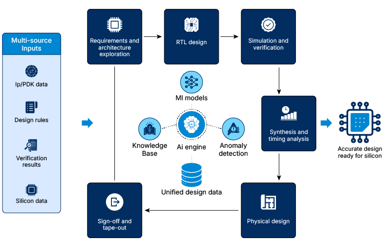
Machine learning models deliver the greatest value by continuously analyzing design data, verification results, and implementation metrics to identify potential issues earlier. Integrating AI models improves quality validation and helps engineering teams design chips accurately before tape-out.
AI prioritizes verification where risks are highest
Modern SoCs generate enormous verification data, making it difficult for engineers to validate every scenario with equal effort. AI identifies high-risk modules that require additional testing by analyzing historical defects, design complexity, and verification coverage. Engineers focus on validation on where failures are most likely, improving accuracy.
AI detects design anomalies before they become costly defects
Machine learning models compare RTL and simulation outputs to identify unusual logic patterns and unexpected design changes. By identifying these anomalies during the development process, engineers can resolve issues before they turn into disaster. Proactively addressing these issues reduces physical design damage and downstream engineering effort.
AI predicts timing and implementation challenges earlier
Timing closure is one of the most challenging phases of chip development. AI can identify paths that violate timing constraints by learning from previous implementation data, timing reports, and routing patterns, before physical implementation begins. With timing-closure insights, engineers can address these risks earlier, reducing late-stage optimization and improving design accuracy.
AI accelerates root-cause analysis for faster design validation
When verification fails, engineers often spend significant time analyzing simulation logs, waveforms, and debug reports to locate the source of the issue. AI correlates information across these engineering artifacts to identify likely root causes, allowing teams to investigate failures more efficiently and resolve recurring design issues with greater accuracy.
AI engineering assistants support engineering decisions across EDA workflows
AI assists engineers by analyzing design documentation, summarizing verification reports, and identifying optimization opportunities. It answers engineering questions using project-specific design data. These AI assistants help engineers by providing contextual recommendations that help teams validate designs more efficiently while maintaining complete engineering oversight.
How does Softweb help semiconductor companies build faster and more accurate chip designs?
Building accurate AI solutions for semiconductor chip design requires high-quality engineering data, semiconductor domain expertise, and continuous model governance. At Softweb, we build AI and machine learning solutions around each client’s engineering workflows, ensuring AI improves engineering accuracy throughout the chip design lifecycle.
Build the right data foundation
We begin by identifying the data the AI model needs. Our team works with semiconductor companies to identify, collect, and prepare engineering data from EDA tools, simulation outputs, verification reports, design documentation, PLM, ERP, and other enterprise systems. By cleaning, standardizing, and contextualizing this data, we create a reliable foundation for training AI models that reflect each customer’s unique chip design environment rather than relying on generic datasets.
Develop AI models tailored to semiconductor engineering
Our team develops customized machine learning solutions as per your business requirements. We build AI models that address challenges such as design verification, timing analysis, design anomaly detection, and engineering knowledge retrieval. Our team trains and validates each model using customer-specific engineering data, enabling more relevant recommendations and higher engineering accuracy. Here’s what that looked like in practice.
45% reduction in design preparation time
Softweb used ComponentIQ to automate reference design search and retrieval for a leading semiconductor solutions provider.
Read the case study →
Integrate AI into existing engineering workflows
We then integrate the AI model into your existing EDA environments, engineering applications, and enterprise platforms. This enables your engineers to adopt AI within familiar workflows, preserving existing engineering investments, and minimizing operational disruption.
Continuously monitor and improve model performance
AI models should evolve with new chip architectures and design methodologies. We continuously monitor model performance and retrain them using new engineering data. Our team also manages model drift to ensure AI recommendations remain accurate, reliable, and aligned with evolving semiconductor design requirements.
Build AI that delivers accuracy and speed together with ComponentIQ
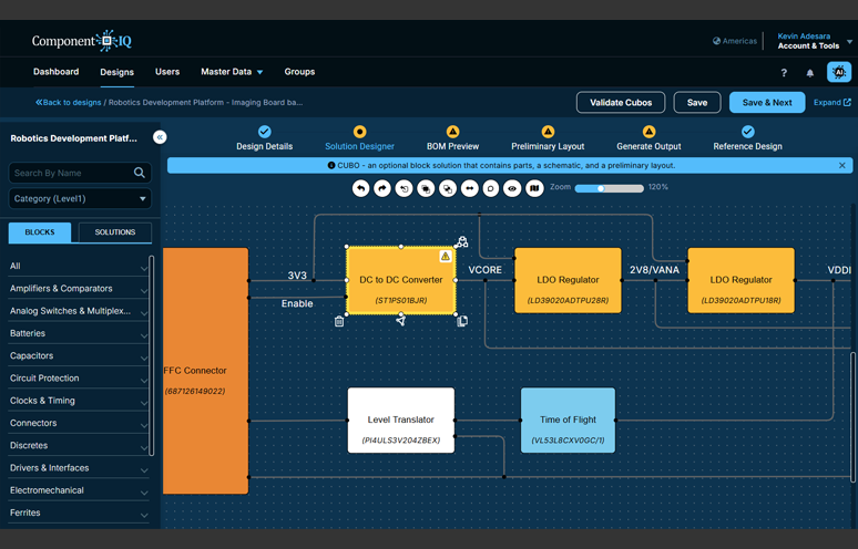
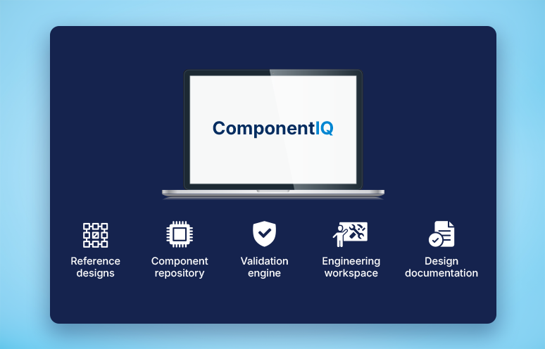
Semiconductor leaders lose time to fragmented tools and validation that occurs too late to catch errors. ComponentIQ solves this with a cloud-based platform that starts every design from a proven reference, validates components in real time, and exports a complete BOM and schematic package.
As more companies adopt similar AI tools, speed alone won’t stay at a competitive edge. McKinsey found that only 5% of semiconductor companies have scaled AI across multiple business domains. Long-term success needs trusted data and smooth EDA integration.
If you’re exploring ways to bring accuracy and speed together in your workflows, ComponentIQ is worth a look.