Achieved 93.7% defect detection accuracy by implementing deep learning solutions for semiconductor wafer manufacturers
Our client is a large-scale manufacturer and distributor of semiconductor wafers. They provide diagnostic and wafer customization services for electronics, biotech, and nanotechnology industries. They collaborated with Softweb Solutions to develop an automated defect detection solution that performed image classification, identified defect patterns, improved accuracy, and reduced human intervention.
 Industry: Semiconductor
  Business type: Enterprise
 - Services: Automatic defect detection
- Technology: Python, TensorFlow, Keras, Azure Blob Storage
Client profile
The client is a large-scale manufacturer and distributor of wafers used in the production of electronic devices like desktops, laptops, smartphones, televisions, washing machines, digital cameras, and refrigerators. They also offer diagnostic services and wafer customization services. They serve clients in the electronics, biotech, and nanotechnology industries. The company is operational for more than five decades and has its head office in the USA, and registered offices in China and Japan.
Technical challenges
Semiconductor wafers are crucial in the electronic world because they serve as the base material for creating electronic components like transistors, resistors, and capacitors. Defect detection is an important part of production as wafers must be checked for quality before rolling out. Our client, being a leading provider of wafers, had to manufacture wafers in huge volumes. They would have faced significant losses in annual revenue due to poor quality control and undetected product defects. Our client struggled with the following technical challenges:
Manual defect detection process
Their manual defect detection process was tedious, time-consuming, and prone to errors that resulted in damaged product reaching customers.
Delay in production
They failed to keep up with high-volume production, creating delays in the manufacturing process and affecting order delivery of ETAs.
High false positive
Their old system was not accurate in distinguishing relevant and irrelevant images. This resulted in poor quality production, which slowed down their operational efficiency.
Inability to fulfill orders
As production was affected due to the above reasons, they were not able to fulfil the demands of their distributors and suppliers on time.
Our solution
We developed an automated defect detection solution using deep learning technology for our semiconductor client to help them identify defect patterns and perform image classification effectively that would fit into existing fab workflows without disruption and improve yield. Our team analyzed the data to understand the root cause of the problem, then observed the position of defects in the wafer images, which gave us insight into the common defect scenarios.
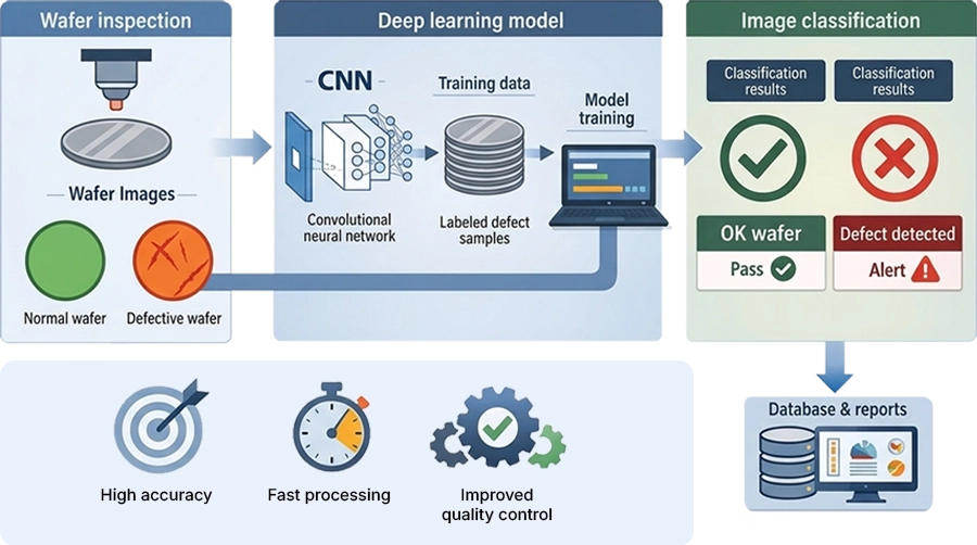
We created data models that examine background pixels and foreground pixels, which helped us to extract pattern features. Deep learning networks require a large amount of data, and we had limited data to train the AI model, so we used Google’s pre-trained TensorFlow Inception CNN Models instead of creating and training the deep neural nets from scratch to save time and data. We evaluated the trained Python model on the new wafer images to calculate its predictive accuracy. Our solution achieved 93.7% defect detection accuracy, and we deployed it successfully to production on an Nvidia GTX 1060 8GB GPU. Our client can now detect defects in early stages of production through image classification, that improved yield and boost operational efficiency.
Identified the position of defects in the wafer images at various locations
Our team analyzed the data to understand the root cause of the problem. We observed the position of defects in the wafer images at various locations, which gave us insight into the common defect scenarios.

Pre-processed of the data and applied the grayscale image segmentation technique
We carried out the pre-processing of the data and applied the grayscale image segmentation technique. Our approach was to carry out detection as a classification task at the pixel level. Therefore, we created data models that examine background pixels and foreground pixels, which helped us to extract pattern features. Deep learning networks require a large amount of data for training. In the case of semiconductor wafers, where defects must not be frequent, the number of non-defective images outweighed the defective images. However, the client provided had a limited set of data, and we solved the imbalanced dataset problem through image augmentation using the Keras Python Library. This helped us to increase the number of samples in our data set using the small data set provided by the client. Further, we divided the enlarged dataset into training and validation data.

By creating and training the deep neural nets from scratch
We decided to use Google’s pre-trained TensorFlow Inception CNN Models instead of creating and training the deep neural nets from scratch to save time and data. Then we fine-tuned the weight parameters using the feature extraction mechanism which included feature creation, feature ranking, and dimensionality reduction. We trained the new classification model written in Python on our dataset to identify defect patterns and predict the label of unseen wafer images in the future.

Validated and deployed the defect detection solutions
We evaluated the trained Python model on the new wafer images to calculate its predictive accuracy. Our solution achieved 93.7% defect detection accuracy, and we deployed it successfully to production on an Nvidia GTX 1060 8GB GPU.

Business goals and measurable outcomes
| Business objective | Business benefit delivered |
|---|---|
| Improved accuracy | Defects can now be automatically detected from the wafer images that improved production accuracy |
| No human involvement | As the defect detection process is automated it immediately identifies defects in the process reducing human error and fake positive |
| Rare event detection | Deep learning technology easily identifies rare defects as the technology continuously learns and evolves from the feedback |
| Reduced memory | Implementing convolutional layer reduced the memory storage requirement |
| Predictive analysis | Using real-time dashboards enables manufactures to predict defects from the images produced |
| Improve production | Automated defect detection enables manufactures to improve yield produced and ROI by identifying defects in the early stage |
Tech stack
- Programming & Frameworks
- Python, TensorFlow, Keras
- AI/ML Techniques
- Deep Learning, Convolutional Neural Networks (CNN), Image Classification
- Data Processing
- Image Preprocessing, Grayscale Segmentation, Data Augmentation
- Model Strategy
- Transfer Learning (TensorFlow Inception Model), Feature Extraction & Optimization
- Storage & Data Handling
- Azure Blob Storage
- Compute Infrastructure
- NVIDIA GTX 1060 GPU (Model Training & Inference)
- Deployment
- Production-Ready ML Model for Automated Defect Detection
- Architecture
- AI-Powered Computer Vision Pipeline for Semiconductor Defect Detection
Similar case studies

Consolidated acquired product catalogs into a unified PIM for a global semiconductor leader

Solved inspection challenges for a semiconductor manufacturer

Empowering wealth management operations with GenAI solutions
Connect Now
Our experts would be eager to hear you.
